
PCB Design
To accommodate our chip and peripheral circuitry, a custom PCB is required. Due to the small-scale of the design, two-layer boards are sufficient. To keep PCB board organized and to help debugging easier, we decide to divide systems into four parts: a RF motherboard, a RF filter board, an LO generation board, and an audio board. The assembled system is shown in Fig.1. During the process, we use DipTrace PCB design software and PCB Minions as our PCB manufacturer.
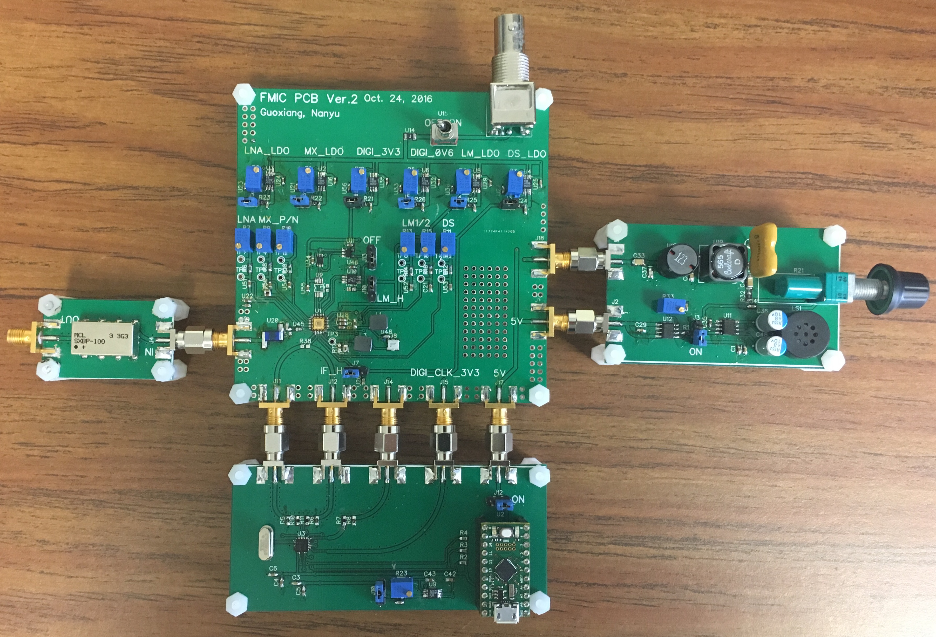
Fig.1 Photo of Assembled Boards
RF Motherboard
The motherboard receives RF signals from the RF filter board, and generates base-band signals to the audio board. It incorporates the designed chip and peripheral circuitries, including LDOs, trimmers, matching networks, IF filters, and base-band processing circuits. Fig.2 presents the layout and the photo of the board.
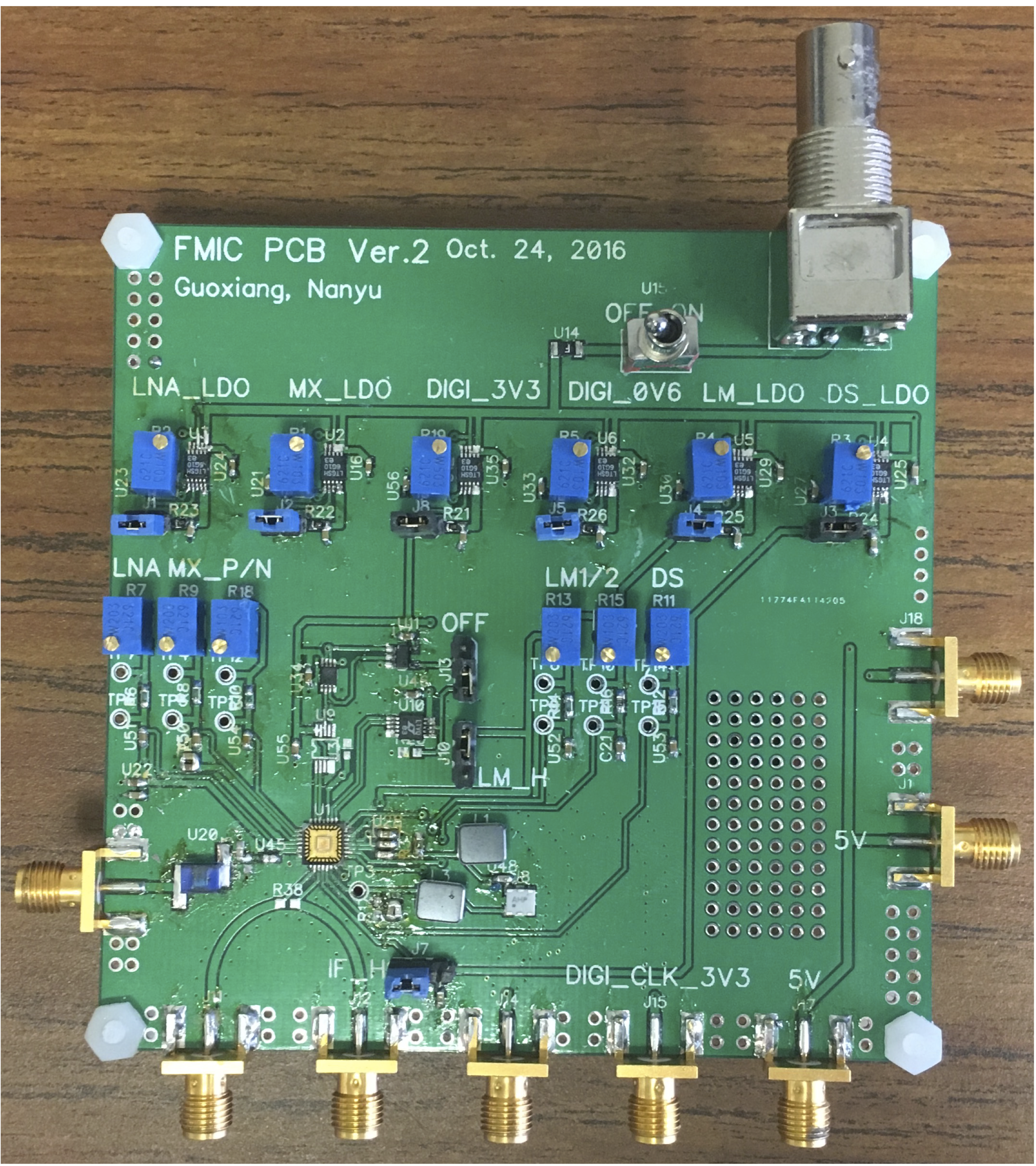

Fig.2 Photo and Layout of RF Motherboard
For the RF matching network, co-planar wave guides are employed with a characteristic impedance of . LineCalc in Keysight ADS is used to synthesize the width of the transmission line. The PCB board characteristics are tabulated in Tab.1.
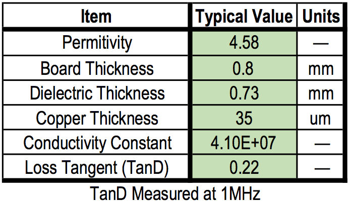
Tab.1 PCB Board Characteristics
For the IF filter network, Murata ceramic filter is employed at the center frequency of 10.7MHz and with the bandwidth of 180kHz. Since the I/O impedance of the filter is , matching networks are required at both the input and output of the filter.
For the LDO array, 6 LDOs from Linear Tech. are employed to provide supply for the chip and the clock generator. Jumpers are added at each output of LDOs for better control and power measurement.
LO Generation Board
The LO generation board provides differential clock signals for the mixer and the single-ended clock signal for the digital demodulator. It employs Si5338 to generate LO signals. There is also an Arduino on the board to interface with Si5338 using I2C protocol. The layout and the photo of the board are shown in Fig.3.
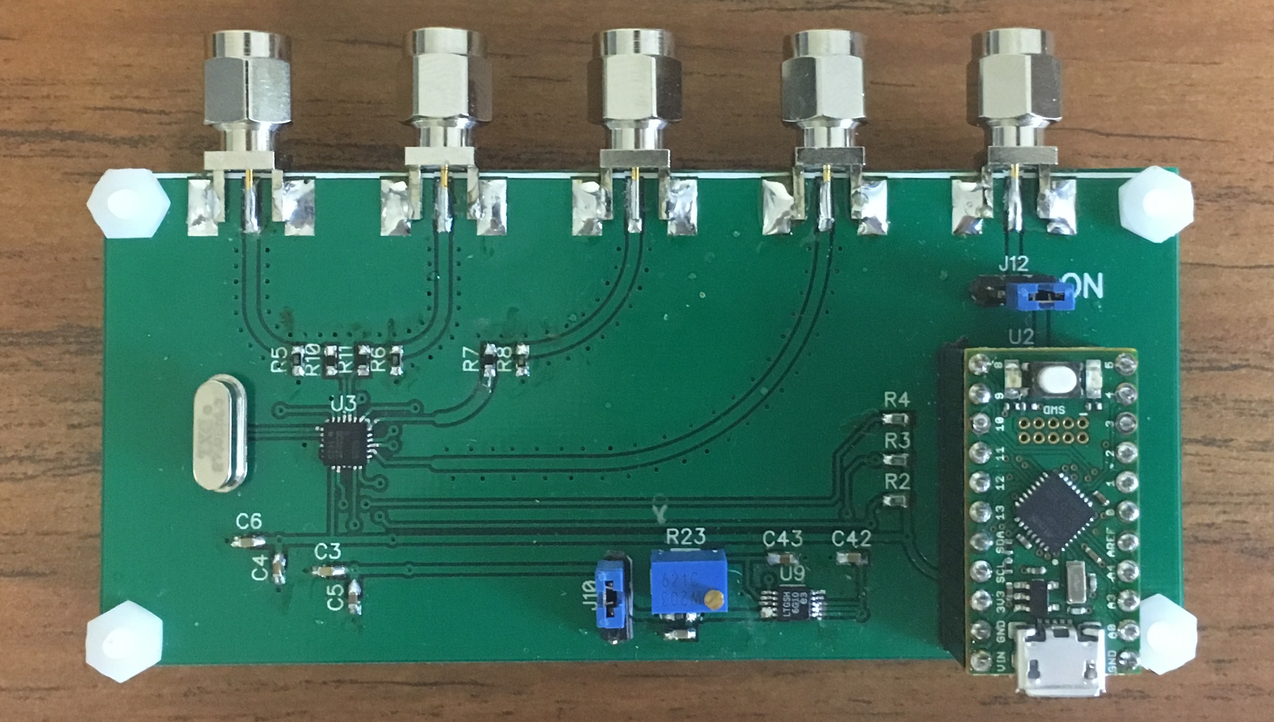
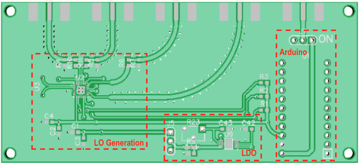
Fig.3 Photo and Layout of LO Generation Board
The typical power supply for both MCU and clock generator is at 3.3V. Since the lowest output voltage of the clock generator is 1.8V, the application note of AN408, is referred to produce a 1.2V differential LO outputs.
Audio Board
The audio board receives the baseband signals, produces audio signals, and plays the music out using an speaker. The board includes an LC low-pass filter, an audio amplifier, and a speaker. The layout and the photo are shown in Fig.4. The filter design guide in Keysight ADS is used to synthesize a fifth-order LC low-pass filter with the cut-off frequency of 20kHz. A class-AB audio-amplifier form Analog Device and an speaker from Pui Audio are employed. A rotary potentiometer is used to perform volume control.
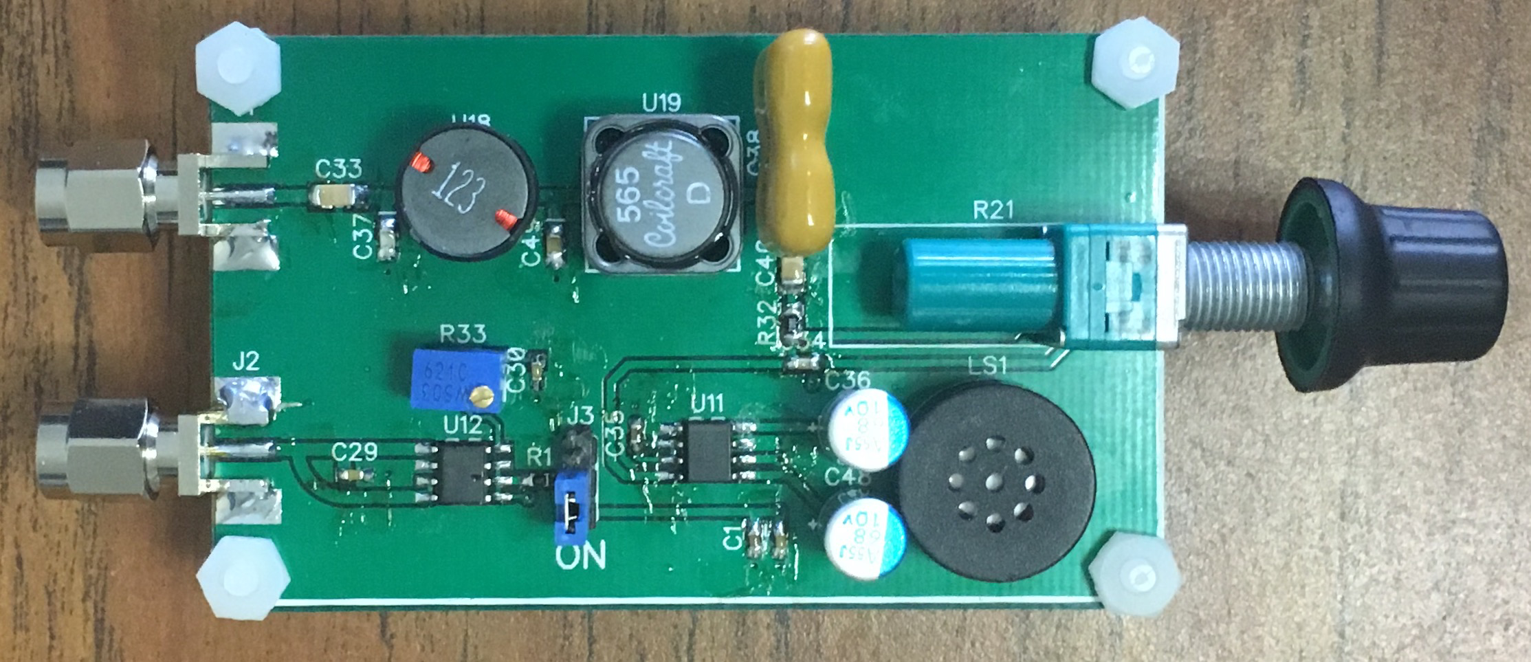
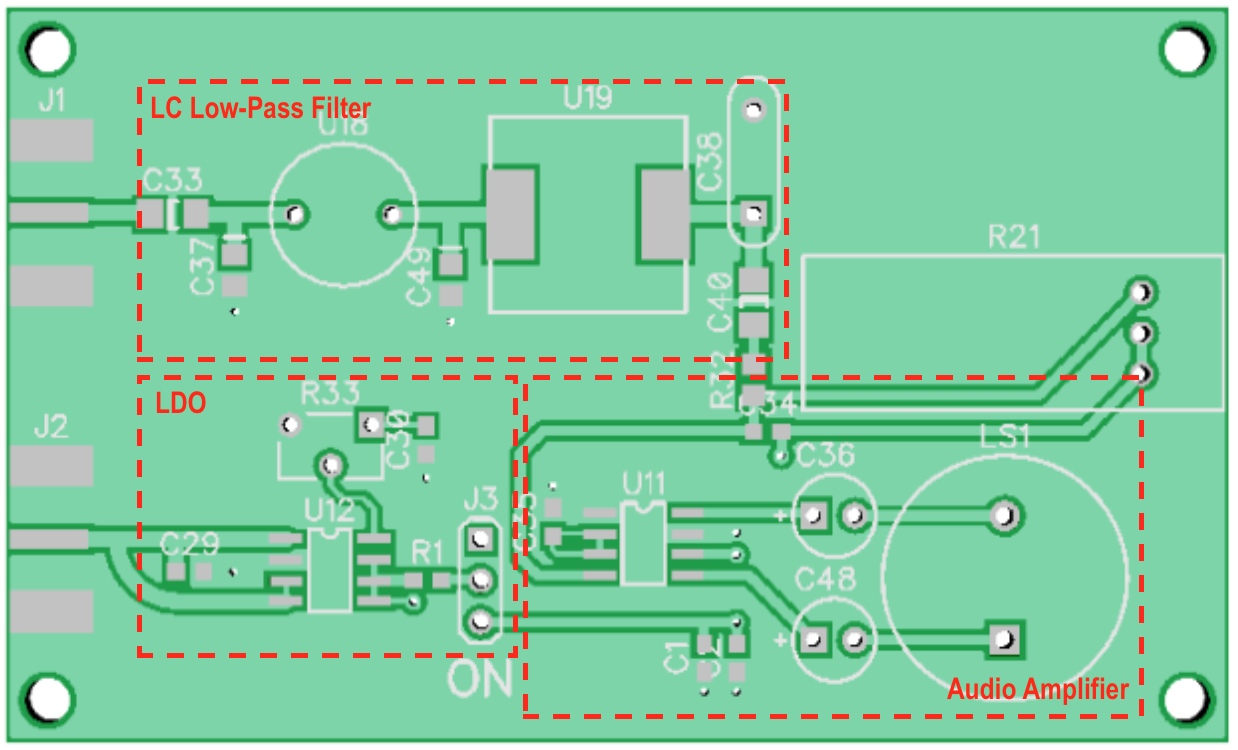
Fig.4 Photo and Layout of Audio Board
RF Filter Board
The RF filter board connects the FM antenna with the motherboard. It includes an FM band-selection filter from Mini-Circuits. Fig.5 shows the layout and the photo of the board.
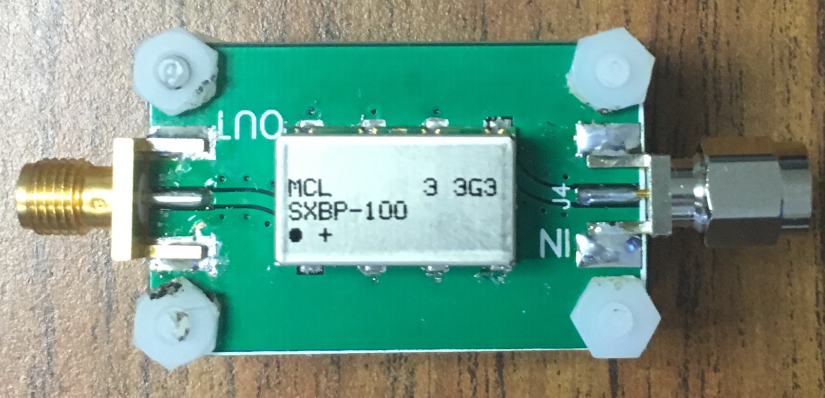
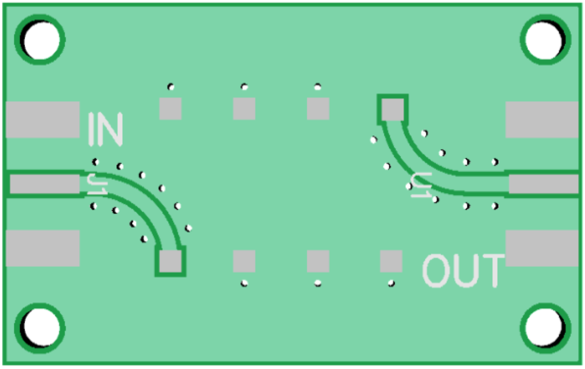
Fig.5 Photo and Layout of RF Filter Board